Difference between revisions of "Project:PCB Making"
(→Notes) |
|||
| Line 130: | Line 130: | ||
== Notes == | == Notes == | ||
| − | Artwork can be printed straight onto a transparency sheet, on a laser printer. Alternatively high street print shops will do the job. | + | Artwork can be printed straight onto a transparency sheet, on a laser printer. Alternatively high street print shops will do the job. One run on the laser might not be dark enough, try printing multiple times on the same sheet to lay down more toner. |
The board was drilled on the Dremel Workstation. | The board was drilled on the Dremel Workstation. | ||
| − | Drill bit; 0.7mm (smallest one) on the workstation plastic drill case, chuck is in the silver dremel case. | + | Drill bit; 0.7mm (smallest one) on the workstation plastic drill case, chuck is in the silver dremel case. [I couldn't find a suitable drill bit or chuck, or silver dremel case for that matter...] |
| − | The UV box | + | The UV box, etching tubs and all chemicals are currently in the left hand metal cupboard (marked etching stuff) at the far end of the dirty room. |
| − | |||
| − | |||
If anyone in interested in making PCBs and needs a hand, let me know. | If anyone in interested in making PCBs and needs a hand, let me know. | ||
[[Category:Projects]] | [[Category:Projects]] | ||
Revision as of 08:31, 5 August 2010
Project maintained by Daniel Sikar ~/ dsikaratgmaildotcom.
Project Brief
Summary
How to make a Printed Circuit Board (PCB) using photoresist laminates.
Overview
This howto is intended as a module, aimed at providing building blocks to emulate and extend projects such as the Benito 7, Nanduino and Teensy.
Equipment
There is an ongoing pledge campaign to improve facilities with a better etch tank
Motivation
PCB making autonomy, although not an absolute necessity in this day and age, is helpful.
Once an electronic prototype is working on a breadboard, the next logical step is to firm up all components on a PCB, where they are less likely to come apart.
Bringing electronic designs to life engenders spatial awareness and can also be fun.
The bigger picture
There are several steps in producing electronic devices. PCB making comes in after the artwork is ready to be transferred and before the components are ready to be soldered onto the board.
There are also alternatives to some of the chemical processes - e.g.
Method
The method described consists of exposing, developing, etching, drilling and tinning a photoresist copper-clad board.
Bill of Materials (BOM)
- Photoresist Copper-clad board Maplin product page (code FA61R).
- Sodium silicate Maplin product page (code AP01B). - full bottle purchased 05-Aug-2010
- Ferric chloride Maplin product page (code XX12N).
- Methylated spirits Wickes product page (code 600343).
- Flux pen Maplin product page (code N63AA).
Additionally:
- Scale
- Tubs
- Mixing and storing vessels
- UV exposure box
- Hammer & punch
- Drill & drill bits
- Gloves (found under the sink)
Steps in a nutshell
Note in this cross section, black in the transparency layer represents a via (trail) on the left and a pad (where a component pin will be soldered) on the right.
1. The artwork (printed onto a transparency) is placed over the photoresist copper-clad board and exposed to UV light. (8 minutes)
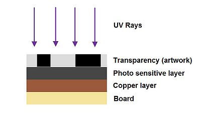
2. The photo sensitive coating weakens as a result of exposure, and is rinsed off with a 10% sodium silicate solution. (1-2 minutes)

3. Copper-clad board is immersed in a 30% ferric chloride solution until etched. (30-40 minutes)

4. Remaining photo sensitive layer is removed with Methylated spirits. This can also be achieved by scrubbing the etched board with wire wool.

5. Board is drilled to allow mounting of Through Hole (TH) components.

6. Flux is applied to copper, which is then tinned.

An additional step is to coat the finished board with an insulating layer which prevents short circuits in case of conductive objects coming in contact with the copper trails. This can be distinguished by a varnish (often green) finish, seen in commercial PCBs.
Clean up
The chemicals can be returned to their respective bottles, and the small residue in the tubs used in the process should be rinsed out in the sink.
Once spent, the sodium silicate solution can be poured down the drain. The ferric chloride on the other hand, must be taken to a Harzadous Disposal Unit, or, deactivated according to this method.
Real life example
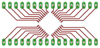
- Artwork, generated by the popular CadSoft Eagle package (.brd file, "top" and "pad" layers shown). The enlarged image represents a TQFP 32 to DIL 32 converter. Print your designed reversed so that the printed side of the transparency can be placed next to the board when exposing to UV. Keeping the toner as close to the board as possible means you can acheive better definition on this traces.
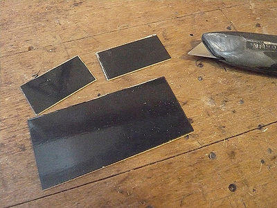
- Cutting board to size, by scoring and snapping.
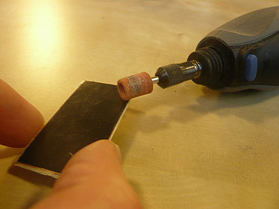
- Finishing the edges, to ensure good contact between transparency and board. Very important step, if any of the edges are raised the UV can get under the transparency and you'll lose definition on thin traces.
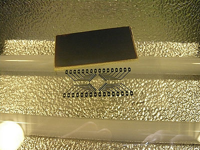
- Preparing for exposure. Double-up transparency for better results, or run through the printer two or three times to put down more toner.
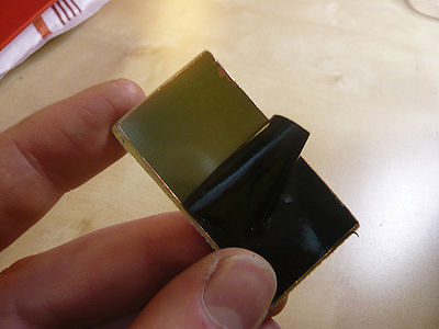
- Peeling off protective layer.
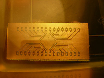
- Expose in the UV box.
- Developing the photoresist in a sodium silicate solution.
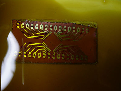
- Etching away the unwanted copper in a ferric chloride solution.
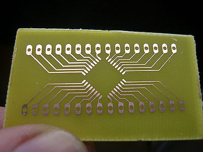
- The etched board.
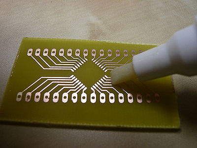
- Applying flux.
Notes
Artwork can be printed straight onto a transparency sheet, on a laser printer. Alternatively high street print shops will do the job. One run on the laser might not be dark enough, try printing multiple times on the same sheet to lay down more toner.
The board was drilled on the Dremel Workstation. Drill bit; 0.7mm (smallest one) on the workstation plastic drill case, chuck is in the silver dremel case. [I couldn't find a suitable drill bit or chuck, or silver dremel case for that matter...]
The UV box, etching tubs and all chemicals are currently in the left hand metal cupboard (marked etching stuff) at the far end of the dirty room.
If anyone in interested in making PCBs and needs a hand, let me know.
