Difference between revisions of "Project:Nanode/Building a Nanode"
| Line 71: | Line 71: | ||
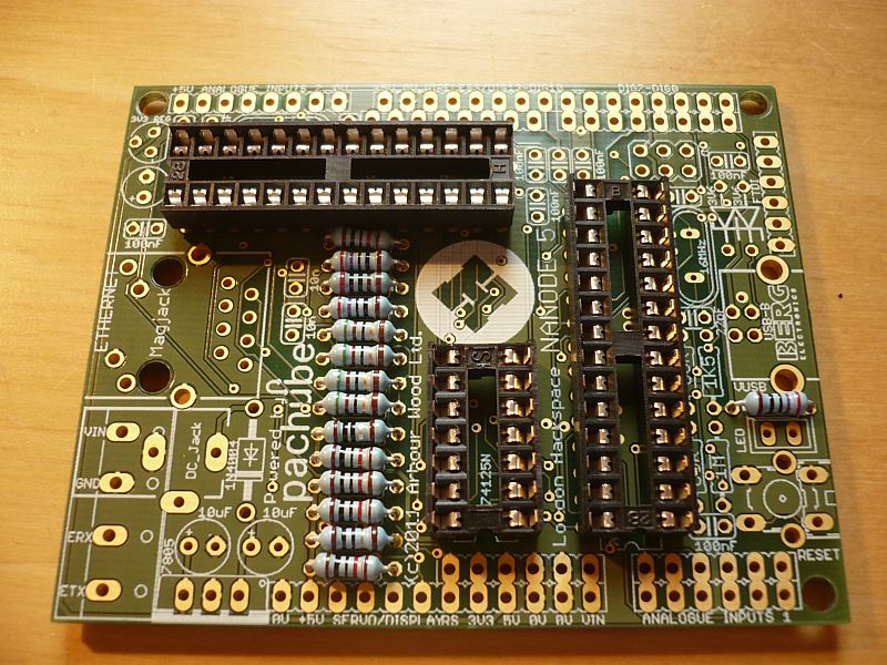
[[File:5_add_ic_sockets.jpg|800px|center|thumb|IC Socket alignment]] | [[File:5_add_ic_sockets.jpg|800px|center|thumb|IC Socket alignment]] | ||
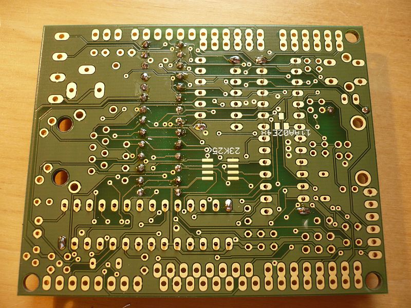
| − | [[File:6_tack_IC_socket_corners.jpg|800px|center|thumb| | + | [[File:6_tack_IC_socket_corners.jpg|800px|center|thumb|Flip the pcb over and tack diagonally opposite corner pins first]] |
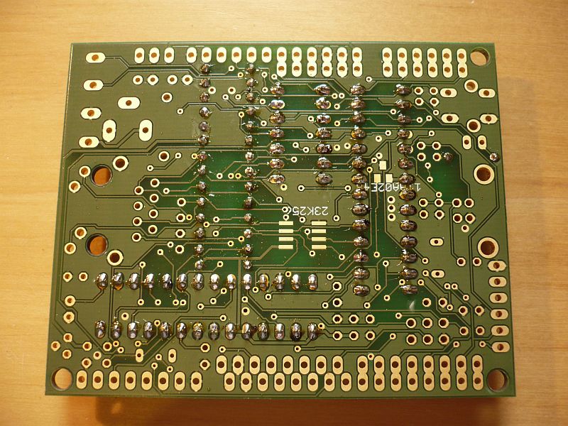
[[File:7_solder_them_in.jpg|800px|center|thumb|Then solder every pin]] | [[File:7_solder_them_in.jpg|800px|center|thumb|Then solder every pin]] | ||
| Line 83: | Line 83: | ||
==Step 9== | ==Step 9== | ||
| − | Add the 25MHz crystal marked 25.00SCA | + | Add the 25MHz crystal marked 25.00SCA. Crystals should be inserted so that the top lies flush with the top of the adjacent IC socket. |
| − | [[File:9_add_25MHz_crystal.jpg|800px|center|thumb|Add the 25MHz crystal]] | + | [[File:9_add_25MHz_crystal.jpg|800px|center|thumb|Add the 25MHz crystal so its flush with the nearby IC socket]] |
| Line 92: | Line 92: | ||
Add the 16MHz crystal marked 16.00SCA | Add the 16MHz crystal marked 16.00SCA | ||
| − | [[File:10_add_16MHz_crystal.jpg|800px|center|thumb|Add the 16MHz crystal]] | + | [[File:10_add_16MHz_crystal.jpg|800px|center|thumb|Add the 16MHz crystal making it flush with the IC socket ]] |
==Step 11== | ==Step 11== | ||
| − | Add the seven 100nF capacitors, colour blue marked 104. There is a spare location for a 100nF capacitor next to pin 1 of the ATmega328 IC. Do not fit any component in this location - just the seven in the picture. | + | Add the seven 100nF capacitors, colour blue and marked 104. There is a spare location for a 100nF capacitor next to pin 1 of the ATmega328 IC. Do not fit any component in this location - just the seven in the picture. |
[[File:11_add_7off_100nF_caps.jpg|800px|center|thumb|Add the blue 100nF ceramic capacitors]] | [[File:11_add_7off_100nF_caps.jpg|800px|center|thumb|Add the blue 100nF ceramic capacitors]] | ||
| Line 121: | Line 121: | ||
==Step 15== | ==Step 15== | ||
| + | |||
Add the FTDI header - a 6 way right angled header on the right hand side of the pcb. Make sure it is straight and level. | Add the FTDI header - a 6 way right angled header on the right hand side of the pcb. Make sure it is straight and level. | ||
| Line 134: | Line 135: | ||
==Step 17== | ==Step 17== | ||
| − | Add the 5V regulator as shown and the 4 way screw terminal block. You need to assemble the two 2 way terminal blocks to make a 4 way - BEFORE you solder to the pcb. | + | Add the 5V regulator as shown and the 4 way screw terminal block. You may need to assemble the two 2 way terminal blocks to make a 4 way - BEFORE you solder to the pcb. |
[[File:18_add_5Vreg_screwterms.jpg|800px|center|thumb|Fit the 5V Regulator and the Screw Terminal Block]] | [[File:18_add_5Vreg_screwterms.jpg|800px|center|thumb|Fit the 5V Regulator and the Screw Terminal Block]] | ||
| Line 140: | Line 141: | ||
==Step 18== | ==Step 18== | ||
| − | Fit the 1N4001 protection diode as shown - noting that the banded end | + | Fit the 1N4001 protection diode as shown - noting that the banded end is lined up with the band on the pcb legend |
[[File:19_add_In4001_diode.jpg|800px|center|thumb|Fit the 1N4001 reverse polarity protection diode]] | [[File:19_add_In4001_diode.jpg|800px|center|thumb|Fit the 1N4001 reverse polarity protection diode]] | ||
| Line 148: | Line 149: | ||
Now - the tricky part. The 3V3 regulator needs to be fitted in a certain way - but not like the pcb symbol. Copy the orientation as in the next 2 pictures. | Now - the tricky part. The 3V3 regulator needs to be fitted in a certain way - but not like the pcb symbol. Copy the orientation as in the next 2 pictures. | ||
| − | [[File:regulator_orientation.jpg|800px|center|thumb|Fit the 3V3 regulator - exactly as shown]] | + | [[File:regulator_orientation.jpg|800px|center|thumb|Fit the 3V3 regulator - turned so it's exactly as shown]] |
[[File:3V3reg_placement.jpg|800px|center|thumb|Fit the 3V3 regulator like this!]] | [[File:3V3reg_placement.jpg|800px|center|thumb|Fit the 3V3 regulator like this!]] | ||
| Line 154: | Line 155: | ||
==Step 20== | ==Step 20== | ||
| − | Now we test the board to make sure that the 5V and 3V3 power supply rails are working OK. We do this before we insert any of the ICs (as more than 60% of the kit value is in the ICs). | + | Now we test the board to make sure that the 5V and 3V3 power supply rails are working OK. We do this before we insert any of the ICs (as more than 60% of the kit value is in the ICs and we don't want a premature fry-up). |
| − | Put the positive probe on pin 14 of the 14 way IC socket and the negative probe on pin 7 of the same socket. | + | Put the positive probe of the meter on pin 14 of the 14 way IC socket and the negative probe on pin 7 of the same socket. |
Insert the FTDI cable with its black wire closest to the centre of the pcb. Look for a voltage close to 5.00V. | Insert the FTDI cable with its black wire closest to the centre of the pcb. Look for a voltage close to 5.00V. | ||
| Line 180: | Line 181: | ||
A similar process for the USB B socket. | A similar process for the USB B socket. | ||
| − | The Red LED is fitted such that the long leg, the anode is inserted in the hole closest to the edge of the pcb. | + | The Red LED is fitted such that the long leg, the anode, is inserted in the hole closest to the edge of the pcb. |
[[File:almost_complete.jpg|800px|center|thumb|Very nearly finished]] | [[File:almost_complete.jpg|800px|center|thumb|Very nearly finished]] | ||
| Line 186: | Line 187: | ||
==Step 22== | ==Step 22== | ||
| − | The ICs can be added | + | Now we come to fit the ICs into their sockets. |
| + | |||
| + | '''Remove the power (FTDI or USB) from the pcb before inserting the ICs!''' | ||
| + | |||
| + | The ICs can be added - making sure you have the correct position and orientation. | ||
| + | |||
| + | Don't get the ATmega328 and the ENC28J60 in the wrong sockets - as that would be bad, quite bad. | ||
The ATmega328 will be supplied pre-programmed with the bootloader. | The ATmega328 will be supplied pre-programmed with the bootloader. | ||
| − | |||
| − | |||
Some ICs will have their pins slightly splayed. This can be fixed by pressing the side of the IC firmly against the bench top until the pins are straight and parallel. | Some ICs will have their pins slightly splayed. This can be fixed by pressing the side of the IC firmly against the bench top until the pins are straight and parallel. | ||
Revision as of 12:05, 2 June 2011
Building a Nanode - in Words and Pictures
Here's how to build up a Nanode as a step by step guide. It should take you a couple of hours.
Step 1
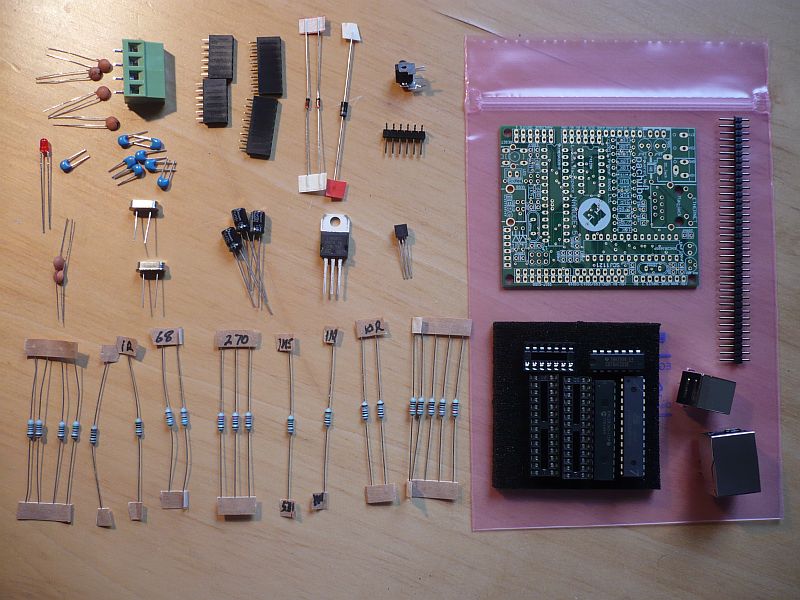
First identify the kit contents
Here you see all the resistors, capacitors, connectors, crystals and ICs needed to make the standard build of Nanode 5.
Everything should be supplied in a pink antistatic plastic "zip" bag.
Step 2
Now orientate the board so that the writing is positioned like this. Note how the component value has been written underneath or close by the component location.
This is the basic starting point for the build sequence. The pcb is built in an orderly sequence starting with the resistors and small components that are low on the board and then working up to the bulkier parts like connectors.
Building a Nanode is just a case of replicating the steps shown in the following picture sequence - no real electronics experience needed - just basic soldering skills.
We start with the resistors that make up the central strip. Resistor leads should be bent close to the resistor body within about 1mm.
A tip for doing this without tools - Hold the resistor between thumb and first-finger, and use the other hand to bend the resistor lead over the thumb nail.
Step 3
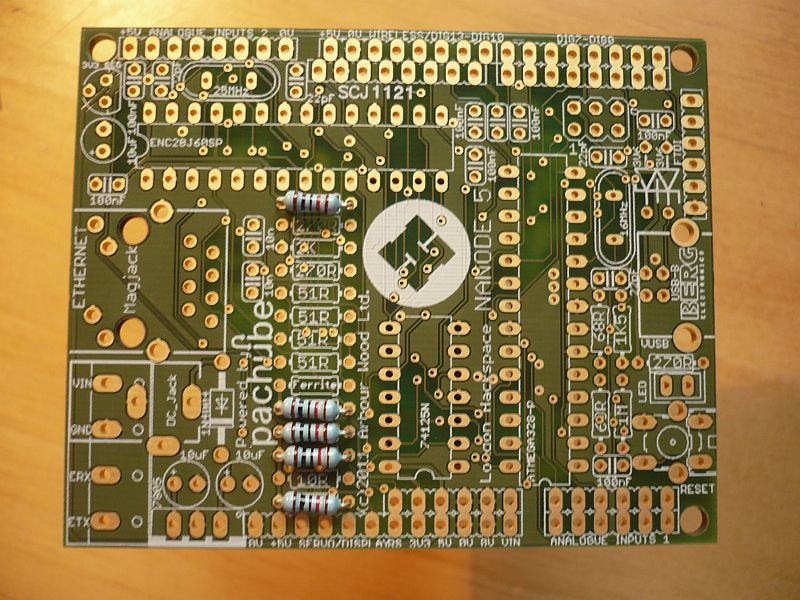
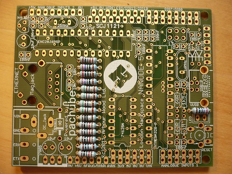
First we add the five 10K resistors - the colour code is Brown Black Black Red (The last band on all resistors is Brown).
Work methodically, - it looks neater if the resistors are all inserted the same direction so that the colour code can be read easily from the left hand side.
Step 4
Now we add the four 51R resistors - the colour code is Green Brown Black Gold.
Step 5
Now we add the three 220R resistors - the colour code is Red Purple Black Black.
Step 6
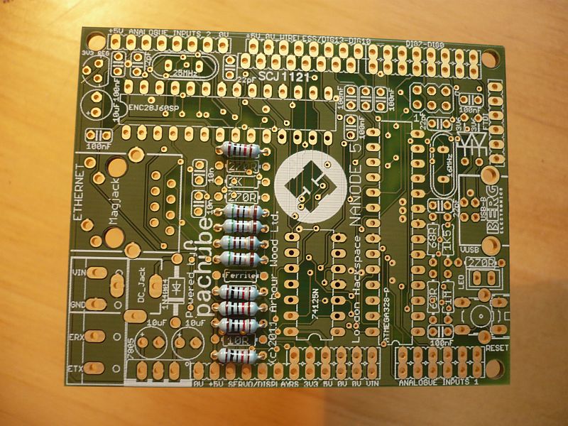
The remaining 1R, 10R and 2K resistors are added.
1R has the colour code Brown Black Black Silver and is fitted in the position marked "ferrite".
The silver and gold colours look very similar in certain light conditions - if in doubt use a multimeter to check the value before you fit it.
10R is Brown Black Black Gold
2K is Red Black Black Brown
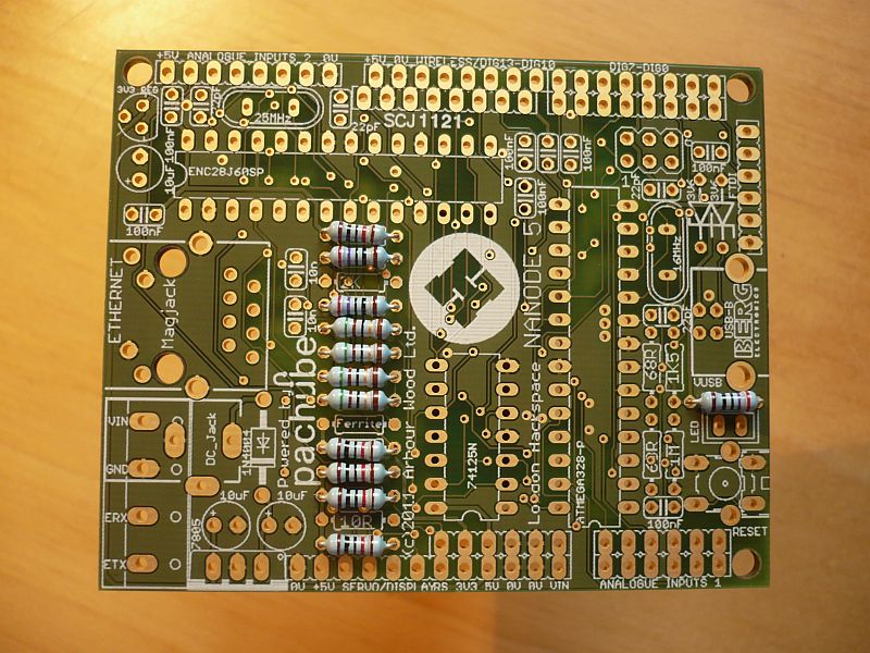
Note - we will not be fitting the two 68R resistors, the 1K5 and the 1M on the right hand side near the USB socket - these are a later virtual USB option - retain them in the kit to be fitted when the software for this option is released.
Step 7
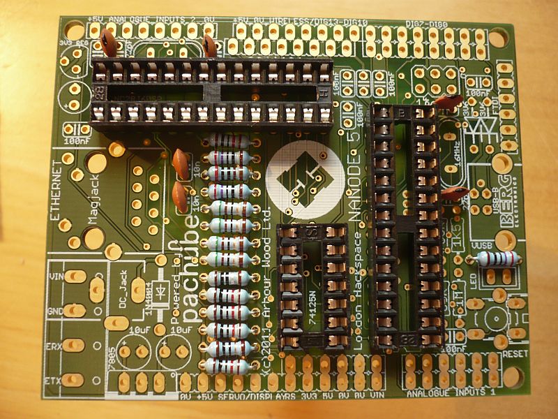
Add the IC sockets making sure that the pin 1 "notch" lines up with the notch in the symbol on the pcb.
It's best to tack diagonally opposite corners to hold the socket in place whilst the rest of the pins are soldered. Make sure they are fitted flat on to the board.
Step 8
Add the four 22pF capacitors marked 22 and with a flash of black paint, and the two 10nF capacitors marked 103
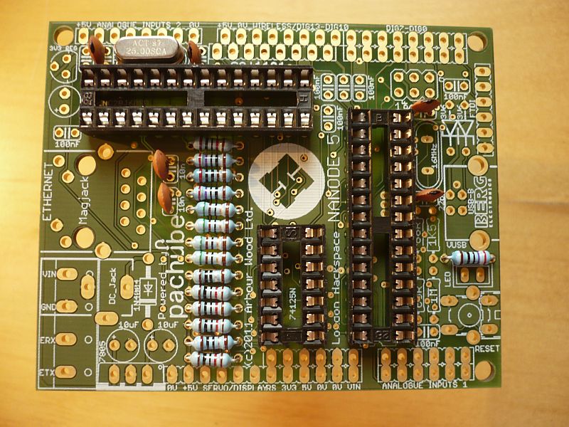
Step 9
Add the 25MHz crystal marked 25.00SCA. Crystals should be inserted so that the top lies flush with the top of the adjacent IC socket.
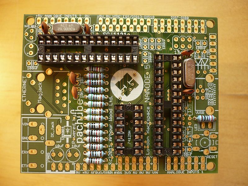
Step 10
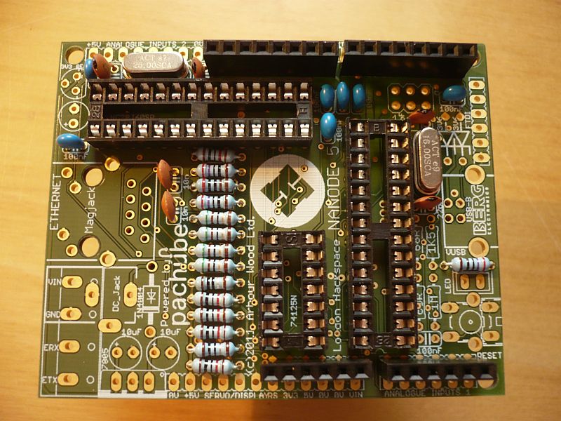
Add the 16MHz crystal marked 16.00SCA
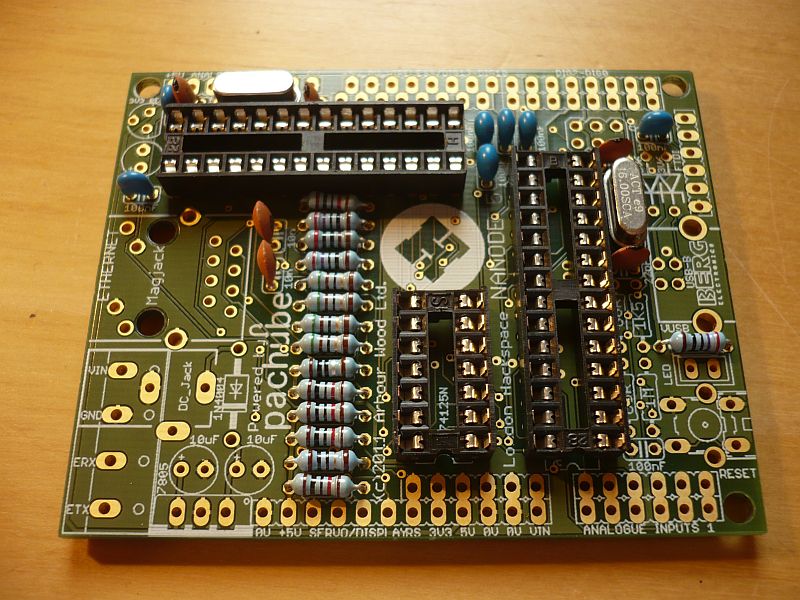
Step 11
Add the seven 100nF capacitors, colour blue and marked 104. There is a spare location for a 100nF capacitor next to pin 1 of the ATmega328 IC. Do not fit any component in this location - just the seven in the picture.
Step 12
Here is the board so far - more than half way.
Step 13
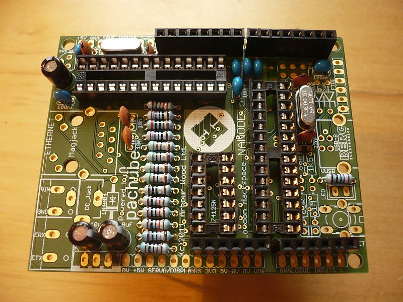
Solder in the "shield" connectors. There are 2 x 6 way and 2 x 8 way SIL sockets. Make sure you get them in the inner lines of holes and that they are fitted straight and vertical. Best to tack one end pin whilst you hold them straight - check the alignment then solder the remaining pins in place.
Step 14
Add the three 10uF electrolytic capacitors - noting that the longer lead is the positive which lines up with the + label on the pcb. You can also confirm the orientation by looking at the position of the white strive (-ve) in the photograph.
Step 15
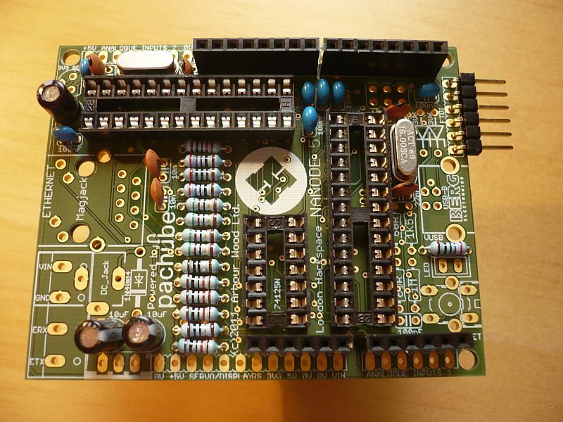
Add the FTDI header - a 6 way right angled header on the right hand side of the pcb. Make sure it is straight and level.
Step 16
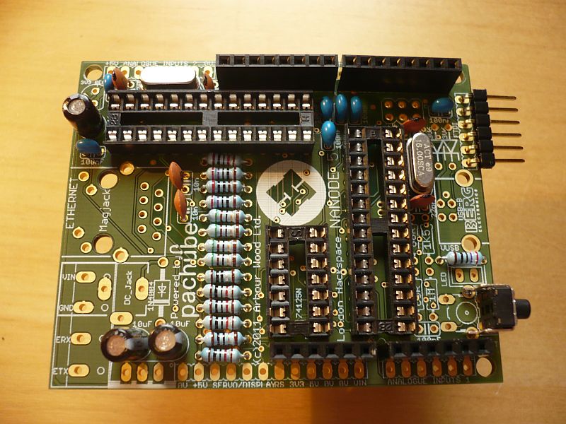
Fit the right angled reset switch
Step 17
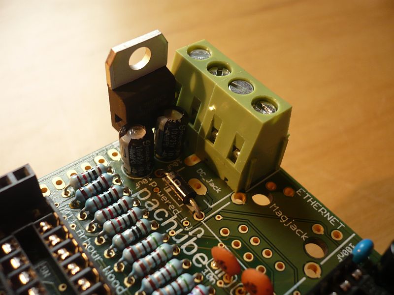
Add the 5V regulator as shown and the 4 way screw terminal block. You may need to assemble the two 2 way terminal blocks to make a 4 way - BEFORE you solder to the pcb.
Step 18
Fit the 1N4001 protection diode as shown - noting that the banded end is lined up with the band on the pcb legend
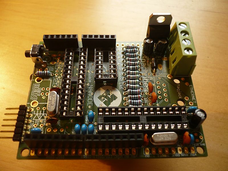
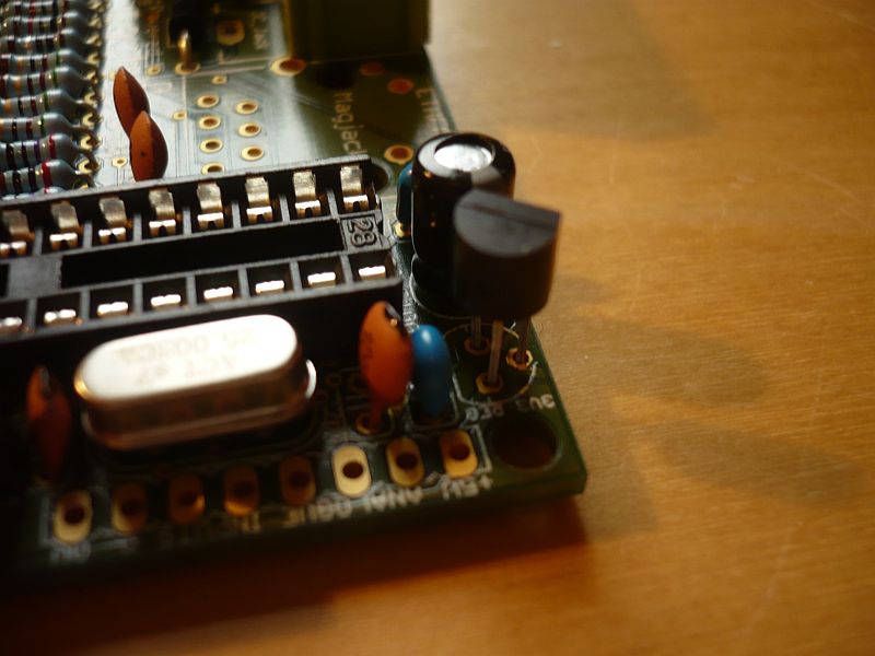
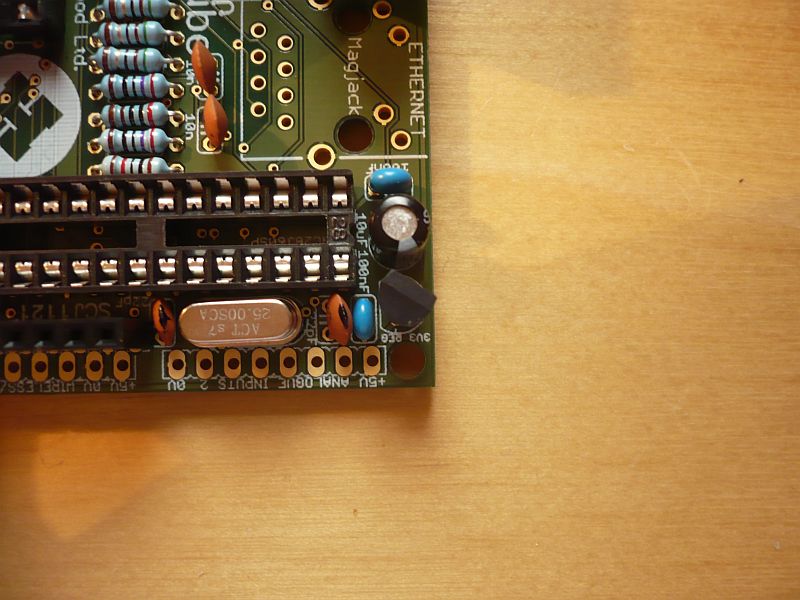
Step 19
Now - the tricky part. The 3V3 regulator needs to be fitted in a certain way - but not like the pcb symbol. Copy the orientation as in the next 2 pictures.
Step 20
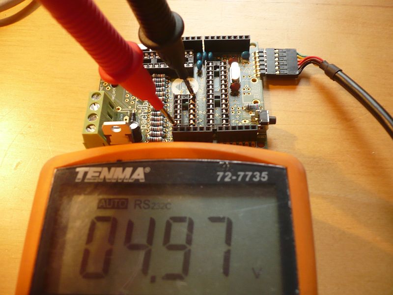
Now we test the board to make sure that the 5V and 3V3 power supply rails are working OK. We do this before we insert any of the ICs (as more than 60% of the kit value is in the ICs and we don't want a premature fry-up).
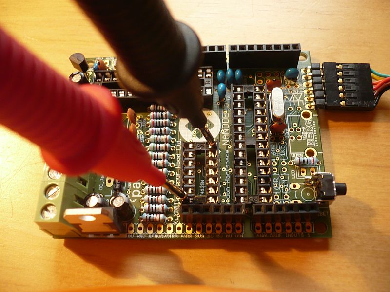
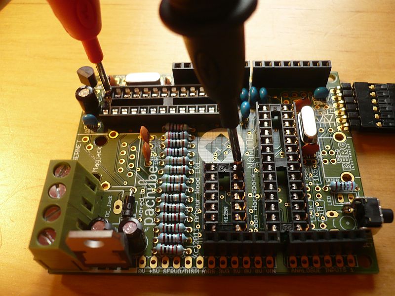
Put the positive probe of the meter on pin 14 of the 14 way IC socket and the negative probe on pin 7 of the same socket.
Insert the FTDI cable with its black wire closest to the centre of the pcb. Look for a voltage close to 5.00V.
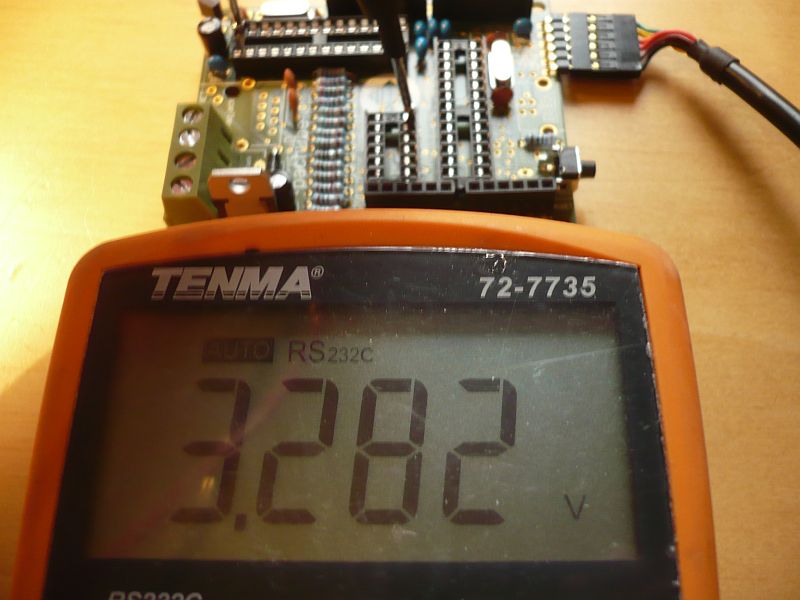
To measure the 3V3, keep the black meter lead on pin 7 of the 14 pin socket and put the red meter probe on pin 28 of the far 28 pin socket as shown. Look for a voltage close to 3.3V
Step 21
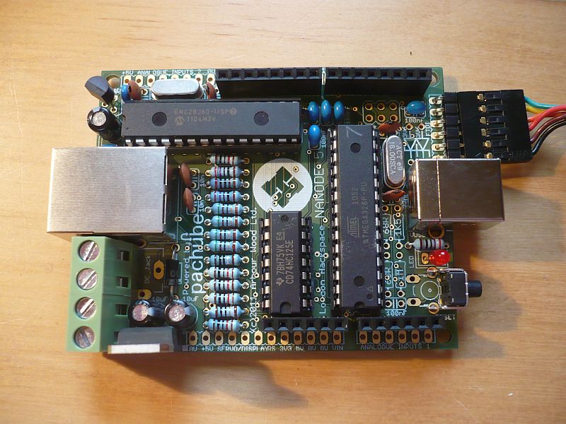
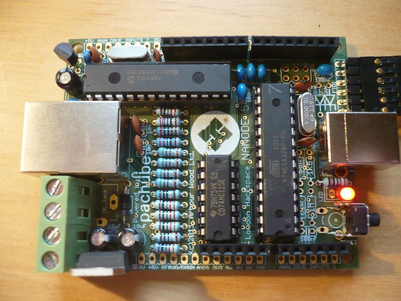
If the voltage tests check out - we can fit the remaining parts - the Mag-jack connector, the USB connector and the Red LED.
The Mag-jack has 12 pins, 2 lugs and 2 prongs to insert, and can be a bit tricky. Line it up carefilly and gently push it home. Make sure all the narrow pins have been correctly inserted through their holes.
Solder in place including the 2 metal prongs.
A similar process for the USB B socket.
The Red LED is fitted such that the long leg, the anode, is inserted in the hole closest to the edge of the pcb.
Step 22
Now we come to fit the ICs into their sockets.
Remove the power (FTDI or USB) from the pcb before inserting the ICs!
The ICs can be added - making sure you have the correct position and orientation.
Don't get the ATmega328 and the ENC28J60 in the wrong sockets - as that would be bad, quite bad.
The ATmega328 will be supplied pre-programmed with the bootloader.
Some ICs will have their pins slightly splayed. This can be fixed by pressing the side of the IC firmly against the bench top until the pins are straight and parallel.
