Project:PCB Making: Difference between revisions
| Line 57: | Line 57: | ||
Note in this cross section, black in the transparency layer represents a via (trail) on the left and a pad (where a component pin will be soldered) on the right. | Note in this cross section, black in the transparency layer represents a via (trail) on the left and a pad (where a component pin will be soldered) on the right. | ||
<br><br> | <br><br> | ||
1. The artwork (printed onto | 1. The artwork (printed onto acetate or paper) is placed over the photoresist copper-clad board and exposed to UV light. (8 minutes) | ||
<br> | <br> | ||
[[File:UV_Exposure.jpg|400px]] | [[File:UV_Exposure.jpg|400px]] | ||
Revision as of 12:07, 10 December 2010
Project maintained by Daniel Sikar ~/ dsikaratgmaildotcom.
| PCB Making
| |
|---|---|
| QR code |
Project Brief
Summary
How to make a Printed Circuit Board (PCB) using photoresist laminates.
Equipment
There is an ongoing pledge campaign to improve facilities with a better etch tank
Motivation
PCB making autonomy, although not an absolute necessity in this day and age, is helpful.
Once an electronic prototype is working on a breadboard, the next logical step is to firm up all components on a PCB, where they are less likely to come apart.
Bringing electronic designs to life engenders spatial awareness and can also be fun.
The bigger picture
There are several steps in producing electronic devices. PCB making comes in after the artwork is ready to be transferred and before the components are ready to be soldered onto the board.
There are also alternatives to some of the chemical processes - e.g.
Another guide can be found here : Mike's electric stuff
Method
The method described consists of exposing, developing, etching, drilling and tinning a photoresist copper-clad board.
Bill of Materials (BOM)
- Photoresist Copper-clad board Maplin product page (code FA61R).
- Sodium silicate Maplin product page (code AP01B). - full bottle purchased 05-Aug-2010
- Ferric chloride Maplin product page (code XX12N).
- Methylated spirits Wickes product page (code 600343).
- Flux pen Maplin product page (code N63AA).
Additionally:
- Scale
- Tubs
- Mixing and storing vessels
- UV exposure box
Recommendation from Imperial College Lab Technician: If you find small specks and holes in the coper then print on normal A4 paper and increase exposure time to 5 mins (as opposed to 12 to 20 seconds with acetate).
- Hammer & punch
- Drill & drill bits
Recommendation from Imperial College Lab Technician: Do not use Tungsten Carbide drills bit with a long shank, they break very quickly. Instead use these with a Dremel and drill press High-speed twist drills with 2.35mm shanks
- Gloves (found under the sink)
Steps in a nutshell
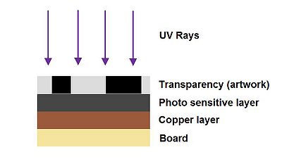
Note in this cross section, black in the transparency layer represents a via (trail) on the left and a pad (where a component pin will be soldered) on the right.
1. The artwork (printed onto acetate or paper) is placed over the photoresist copper-clad board and exposed to UV light. (8 minutes)
2. The photo sensitive coating weakens as a result of exposure, and is rinsed off with a 10% sodium silicate solution. (1-2 minutes)

3. Copper-clad board is immersed in a 30% ferric chloride solution until etched. (30-40 minutes)

4. Remaining photo sensitive layer is removed with Methylated spirits. This can also be achieved by scrubbing the etched board with wire wool.

5. Board is drilled to allow mounting of Through Hole (TH) components.

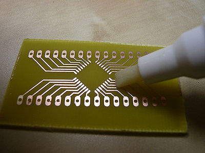
6. Flux is applied to copper, which is then tinned.

An additional step is to coat the finished board with an insulating layer which prevents short circuits in case of conductive objects coming in contact with the copper trails. This can be distinguished by a varnish (often green) finish, seen in commercial PCBs.
Clean up
The chemicals can be returned to their respective bottles, and the small residue in the tubs used in the process should be rinsed out in the sink.
Once spent, the sodium silicate solution can be poured down the drain. The ferric chloride on the other hand, must be taken to a Harzadous Disposal Unit, or, deactivated according to this method.
Real life example
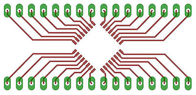
- Artwork, generated by the popular CadSoft Eagle package (.brd file, "top" and "pad" layers shown). The enlarged image represents a TQFP 32 to DIL 32 converter. Print your design reversed so that the printed side of the transparency can be placed next to the board when exposing to UV. Keeping the toner as close to the board as possible means you can achieve better definition on these traces.
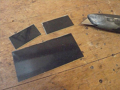
- Cutting board to size, by scoring and snapping - Note the LHS now has a metal sheet cutter which makes this method antiquated.
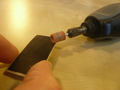
- Finishing the edges, to ensure good contact between transparency and board. Very important step, if any of the edges are raised the UV light can get under the transparency and you'll lose definition on thin traces.
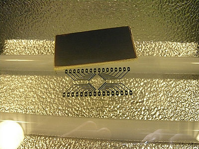
- Preparing for exposure. Double-up transparency for better results, or run through the printer two or three times to put down more toner. Note in Tried and Tested settings, good results were obtained by printing on paper.
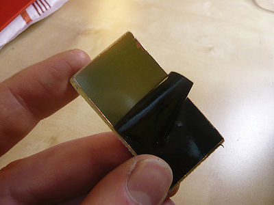
- Peeling off protective layer.
- Expose in the UV box.
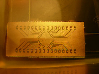
- Developing the photoresist in a sodium silicate solution.
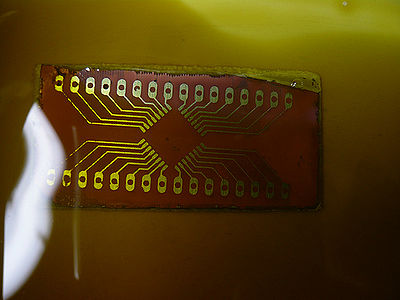
- Etching away the unwanted copper in a ferric chloride solution.
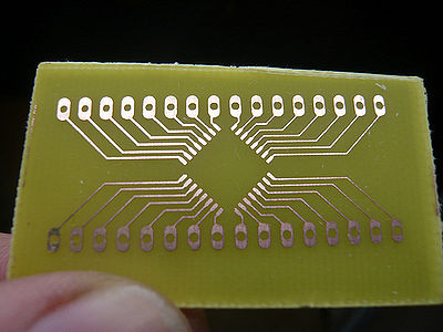
- The etched board.
- Applying flux.
- Tinning
TODO
Notes
Artwork can be printed straight onto a transparency sheet, on a laser printer. Alternatively high street print shops will do the job. One run on the laser might not be dark enough, try printing multiple times on the same sheet to lay down more toner.
The best medium for printing artwork on a laser is tracing paper as it has much better toner adhsion than transparency film and works fine with just one pass - it needs to be fairly thick, at least 90GSM to avoid crinkling in the fuser. A few years ago I wrote this extensive guide to making good PCBs : www.electricstuff.co.uk/pcbs.html
The board was drilled on the Dremel Workstation. Drill bit; 0.7mm (smallest one) on the workstation plastic drill case, chuck is in the silver dremel case. [I couldn't find a suitable drill bit or chuck, or silver dremel case for that matter...]
The UV box, etching tubs and all chemicals are currently in the left hand metal cupboard (marked etching stuff) at the far end of the dirty room.
If anyone in interested in making PCBs and needs a hand, there are now 3 members of the Hackspace etching PCBs in loco - Daniel (dsikar), Solexious and Meurig, all willing to help, I am sure.
Tried and Tested Settings
pingbat & samthetechie 14-Oct-2010
- Plain paper used, run through the printer once. Tried to run it through the printer more than once but alignment was crap.
- 5 minute exposure in the UV box.
- 2 minute developing of the photoresist in the sodium silicate, do not leave it any longer than this, we were tempted and wasted 2 boards.
- We used Maplin Clear Etchant, it was already in the bottle and seemed to work fine although it was quite slow. The tank was agitated using the servo and rocker someone devised, a modified version of the Arduino Servo Sweep example sketch was used.
- We used scales to make up the Sodium Silicate, the scales are in the Multimeter box as of the 14th.
- Results were quite good, nice resolution, might try less than 2 minutes in the developer. Thanks to Muerig and some other kind soul, we have the materials to make Copper Chloride which should be much faster than the clear etchant and can be regenerated so we should never run out.
Meurig - 04-Aug-2010
- Laminate: transparency 'borrowed' from work, run through a laser printer three times on enhanced quality mode, black and white (obviously).
- Board: Maplin SRBP Pre-Sensitised Copper-Clad Board [JP56L]
- Exposure time: Warmed up the UV unit for 2 mintues before starting, then exposed board for 2.5 minutes. Took some care to be quick between peeling and exposing, but wasn't anal about it.
- Developing solution: Maplin Universal PCB Developer [AP01B] made up by eye to approx 10%? was made up by Oni the night before so I'm not sure. Very much room temperatures.
- Developing time: Took about a minute, was really obvious that it was working.
- Etching solution: Maplin clear etchant, I can't find it on the website but it wasn't ferric chloride, again made up by Oni the night before so room temperature.
- Etching time: This took a while, went much faster if I was agitating the solution. Somewhere between 20 and 40 minutes (I was having dinner so didn't really keep track). Heating the solution might speed this up but I wouldn't really want to put in the microwave.
- Removing exceess photoresist: I hadn't read the thing above about white spirit so I just exposed the whole board again (without laminate) for about a minute and ran it through the developer again, worked well but I'll try white spirit next time.
Meths is also good, and less oily & smelly than WS. You need to leave it on for a min or so, then wipe off with paper towel.
- Protective layer: I just covered the whole board with a flux pen (donated by
AdrianFarnell, left by the box of sharpies).
- Addendum: My first board was ruined by leaving a lip where I'd cut it (hacksaw). Always make sure the board is perfectly flat! I left some developer and etchant in the trays since I'm sure they'd by good for a few more runs and I wasn't sure how to dispose of them.
