PCB etching instructions: Difference between revisions
No edit summary |
(Converted the old inline graphviz code to svg) |
||
| (86 intermediate revisions by 20 users not shown) | |||
| Line 1: | Line 1: | ||
'''!!! This is the canonical guide on how to etch PCBs at the LHS !!! ''' | |||
Note : see '''[[Pcb]]''' for other references | Note : see '''[[Pcb]]''' for other references | ||
== | == PCB Etching Process == | ||
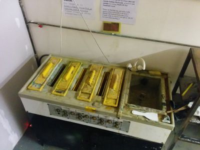
[[File:Pcb-etching-tank.jpg|400px|thumb|right|The PCB etching tank]] | |||
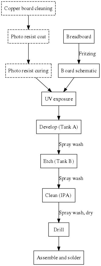
Here's the overall process for producing PCBs @ LHS | |||
'''!!! Please use a small test sample to develop and etch so to avoid wasting time and money !!! ''' | |||
[[File:Etchingprocess.svg]] | |||
=== Photo Sensitive Board === | |||
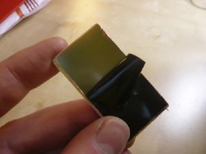
[[File:Peeling_protective_layer.jpg|right|thumb]]It is possible to sensitise your own board by getting a coper clad board, cleaning and coating it with photo-resist and allowing it to cure. However it's vastly easier just to buy some. | |||
See [[Pcb_etching_instructions#Results_people_found_with_materials.2Fcompounds]] for a list of known good materials. | |||
You may want to try: | |||
* [http://www.rapidonline.com/tools-equipment/photoetch-pcb-29445 Photoetch PCB (Rapid)] | |||
* [http://www.megauk.com/pcb_laminates.php FPC 16] (various options there, FPC 16 seems to be the cheapest) | |||
'''NOTE''' : the developer is from Mega Electronics, also sold through Rapid. It works well with photo PCB material from the same source. '''It does ''NOT'' work with Maplin photo material !''' | |||
=== Printing Board Schematic === | |||
[[File:PaperPrint.jpg|right|thumb]] | |||
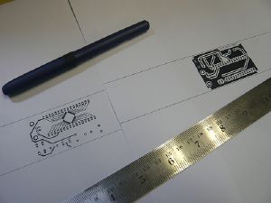
Plain paper works surprisingly well! The printers at the space do a good job. | |||
If you use eagle, you can use the print option (as opposed to exporting an image). Print on normal paper first and check dimensions on some components. | If you use eagle, you can use the print option (as opposed to exporting an image). Print on normal paper first and check dimensions on some components. | ||
Some people get better (resolution mostly, especially for SMT designs) results with acetate, but this needs to be special laserable acetate (which we have, kept with the UV Exposure kit!). '''Do ''NOT'' use normal transparency!''' Melting a sheet onto a fuser is expensive! | |||
If you want to get really upmarket, you could try [http://www.megauk.com/artwork_films.php Mega LaserStar] transfer film (for printing with a laser printer of some sort). Hugely expensive, but does take on plenty toner and produces excellent results. Note from [[User:padski|Paddy]] I highly recommend Laserstar paper, I get perfect results every time, but yes it's £8 for 10 sheets.. | |||
==== Double Sided Boards ==== | |||
[[File:PCB_Artwork_pocket.jpg|right|thumb]] | |||
There's a couple of extra steps required for two-sided boards: | |||
* Print both sides out on separate sheets (or cut one sheet in half), '''one of them mirrored''' | |||
* Align the two sheets and staple them together to retain registration | |||
* Cut them to size so that they are slightly smaller than your photo PCB material. | |||
* Remove the protective film on both sides, place the PCB between the two transparencies leaving a slight overhang, and '''tape the PCB to the transparency ''' so it does not move when you flip it during exposure! | |||
See also [[Project:PCB_Making#Double_sided_boards|Double sided boards]] | |||
=== Spray Resist === | |||
Both Electrolube PRP + Kontakt Chemie Positiv work well, with an exposure time of 6 mins. The board needs to be perfectly clean (superfine steel wool), and evenly + lightly sprayed. Note PRP often clogs its own nozzle and wastes most of the can. No such issue with Positiv. Both require the seno type (not NaOH) developer. | |||
=== UV Exposure === | |||
[[File:Developing photoresist.jpg|right|thumb]] | |||
Use the [[Equipment/UV_Exposure_Box|UV Exposure Box]] to expose a photosensitve board. | |||
Make sure your print is the right way round so that your board isn't back to front when it's etched! | Make sure your print is the right way round so that your board isn't back to front when it's etched! | ||
| Line 15: | Line 61: | ||
5 minutes with acetate and something like 15 with paper. The uv board should look green with faint lighter green traces where your traces are. | 5 minutes with acetate and something like 15 with paper. The uv board should look green with faint lighter green traces where your traces are. | ||
== | Ensure that there are no creases or folds, and that your paper/film is perfectly flat against the photo board! | ||
=== Developing === | |||
[[File:TQFP32 DIL32 PhotoresistDevelopment.jpg|thumb|right]] | |||
Put the board in the developer ([[Equipment/PCB_etch_station#1st_Tank_-_Developer|tank A]]). Developer does not need to be heated to above room temperature to remain effective. Developing should take around 30 seconds to a minute or so - but check on the board to see when it is complete. All of the copper to be removed should be exposed, and only your tracks should remain coloured ( probably green for UV exposure board). | |||
You may wish to give the board a rinse (using the integrated spraying slots in the etching station) after this stage. | |||
=== Etch === | |||
[[File:Etching.jpg|thumb|right]] | |||
The Cupric Chloride etchant is in [[Equipment/PCB_etch_station#2nd_Tank_-_Etchant|tank B]] | |||
Check the colour of the liquid - if it's bright green you're good to go. Otherwise the solution may need aerating for a few minutes before use. | |||
Follow instructions on the notice, but the board is done when all the exposed copper is removed. The balance is removing too much copper and getting breaks in traces vs not enough and some small closely laid traces may have bridges. You are looking for clean edges to your traces - not wobbley "chewed" looking edges (which could indicate you etched for too long, not long enough, or that your exposure wasn't crisp enough). This can take anywhere between 10 and 30 minutes. | |||
After this stage you should rinse the board in water for at least 60 seconds (using the integrated spraying slots in the etching station) before touching it with your hands, transferring to the next tank to begin stripping the photo resist. | |||
=== Stripper === | |||
[[File:Etched.jpg|thumb|right]] | |||
The stripper is in [[Equipment/PCB_etch_station#3rd_Tank_-_stripper|Tank C]] | |||
The stripper removes the photo-resist left over after etching. Use the stripper for the specified time then scrub the black off and you should have nice copper traces! Use a multimeter to check for bridges. | |||
After this stage, you may want to rinse the PCB in clean water using the integrated spraying slots, and then IPA. | |||
=== Milling / Drilling === | |||
[[File:Dremelwor-1397100593-14231.jpg|right|thumb|100px]] | |||
Normal drill press probably not ideal (not immune enough to wandering!). | |||
You could use the [http://www.ebay.co.uk/itm/Dremel-220-01-Workstation-Rotary-Tool-Multi-Purpose-Drill-Press-/271486781801?_trksid=p2054897.l5658 Dremel stand] (on the shelf outside the wood workshop) to drill holes more precisely. | |||
May not have the original dremel, but other (green and blue) rotary tools fit as well. | |||
At this point, you could do any number of finishing options (milling, tinning, soldermask, silkscreen, laquer etc etc). But to aid in the application of solder, you may want to give it a quick brush with some steel wool. | |||
== | === Test / Assembly === | ||
If you're doing a double sided board, you'll need to solder up your vias first (we have no through hole plating facilities). A bit of solid core wire works well for this. | |||
== See also == | == See also == | ||
[[Project:PCB_Making|More info on the process, including photos of an SMT breakout board]] | |||
[[Project:DIY_PCB_Making]] | [[Project:DIY_PCB_Making]] | ||
[[ | == Results people found with materials/compounds == | ||
{| class="wikitable" | |||
!| Name | |||
!| Date | |||
!| PhotoResist source (Rapid photo resist spray/pre sentesized deluxe board?) | |||
!| UV exposure stencil used (paper/acetate?) | |||
!| Exposure time (minutes) | |||
!| Develop time (minutes) | |||
!| Etch time (minutes) | |||
!| Notes | |||
|- | |||
| [[User:mentar|mentar]] | |||
| 14/10/2014 | |||
| [http://uk.farnell.com/kelan/141300/pcb-photo-resist-s-s-100x160mm/dp/141300 Kelan presentesized] | |||
| Transparency | |||
| 3 | |||
| 1-2 | |||
| 8 | |||
| Debugging issues with [http://uk.farnell.com/mega/3204911/pcb-fr4-100x160-ss/dp/3204911?Ntt=320-4911 microtrack boards] | |||
|- | |||
| [[User:mentar|mentar]] | |||
| 3/4/2014 | |||
| [http://uk.farnell.com/kelan/149054/pcb-plain-s-s-100x160mm/dp/149054 Farnell presentesized epoxy glass FR4] board | |||
| Plain paper | |||
| 2 | |||
| 5 | |||
| 12 | |||
| First run in the new space | |||
|- | |||
| Miguel | |||
| 13/5/2014 | |||
| white, single sided presentesized board (space stock) | |||
| Laserable acetate supplied and printed on by [https://plus.google.com/103531632793458744844/about?hl=en local printshop] (£1.50) | |||
| 3 | |||
| 1.5 | |||
| 8 | |||
| Professionally printed acetate | |||
|- | |||
| [[User:jasiek|jasiek]] | |||
| 19/06/2015 | |||
| [http://www.ebay.co.uk/itm/271739145882 Generic PCB from eBay] | |||
| Xerox Performer universal paper | |||
| 15 | |||
| 0.5 | |||
| 20 | |||
| Did not work. Paper blocking UV? | |||
|- | |||
| [[User:jasiek|jasiek]] | |||
| 19/06/2015 | |||
| [http://www.ebay.co.uk/itm/271739145882 Generic PCB from eBay] | |||
| Laser acetate sheet | |||
| 5 | |||
| 0.5 | |||
| 20 | |||
| Worked great | |||
|- | |||
| [[User:levidhuyvetter|levidhuyvetter]] | |||
| 02/08/2015 | |||
| [http://uk.farnell.com/webapp/wcs/stores/servlet/ProductDisplay?catalogId=15001&langId=44&urlRequestType=Base&partNumber=141300&storeId=10151 KELAN 141300 PCB] | |||
| Plain paper from laser printer | |||
| 6 | |||
| 5 | |||
| 18 | |||
| With fresh developer. | |||
|} | |||
[[Category:PCB making]] | |||
[[Category:Guides]] | |||
Latest revision as of 22:44, 8 June 2019
!!! This is the canonical guide on how to etch PCBs at the LHS !!!
Note : see Pcb for other references
PCB Etching Process
Here's the overall process for producing PCBs @ LHS
!!! Please use a small test sample to develop and etch so to avoid wasting time and money !!!
Photo Sensitive Board
It is possible to sensitise your own board by getting a coper clad board, cleaning and coating it with photo-resist and allowing it to cure. However it's vastly easier just to buy some.
See Pcb_etching_instructions#Results_people_found_with_materials.2Fcompounds for a list of known good materials.
You may want to try:
- Photoetch PCB (Rapid)
- FPC 16 (various options there, FPC 16 seems to be the cheapest)
NOTE : the developer is from Mega Electronics, also sold through Rapid. It works well with photo PCB material from the same source. It does NOT work with Maplin photo material !
Printing Board Schematic
Plain paper works surprisingly well! The printers at the space do a good job.
If you use eagle, you can use the print option (as opposed to exporting an image). Print on normal paper first and check dimensions on some components.
Some people get better (resolution mostly, especially for SMT designs) results with acetate, but this needs to be special laserable acetate (which we have, kept with the UV Exposure kit!). Do NOT use normal transparency! Melting a sheet onto a fuser is expensive!
If you want to get really upmarket, you could try Mega LaserStar transfer film (for printing with a laser printer of some sort). Hugely expensive, but does take on plenty toner and produces excellent results. Note from Paddy I highly recommend Laserstar paper, I get perfect results every time, but yes it's £8 for 10 sheets..
Double Sided Boards
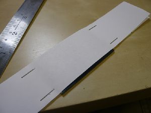
There's a couple of extra steps required for two-sided boards:
- Print both sides out on separate sheets (or cut one sheet in half), one of them mirrored
- Align the two sheets and staple them together to retain registration
- Cut them to size so that they are slightly smaller than your photo PCB material.
- Remove the protective film on both sides, place the PCB between the two transparencies leaving a slight overhang, and tape the PCB to the transparency so it does not move when you flip it during exposure!
See also Double sided boards
Spray Resist
Both Electrolube PRP + Kontakt Chemie Positiv work well, with an exposure time of 6 mins. The board needs to be perfectly clean (superfine steel wool), and evenly + lightly sprayed. Note PRP often clogs its own nozzle and wastes most of the can. No such issue with Positiv. Both require the seno type (not NaOH) developer.
UV Exposure
Use the UV Exposure Box to expose a photosensitve board.
Make sure your print is the right way round so that your board isn't back to front when it's etched!
5 minutes with acetate and something like 15 with paper. The uv board should look green with faint lighter green traces where your traces are.
Ensure that there are no creases or folds, and that your paper/film is perfectly flat against the photo board!
Developing
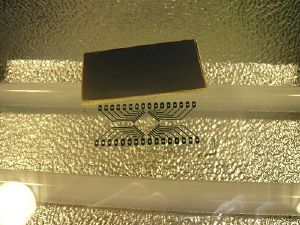
Put the board in the developer (tank A). Developer does not need to be heated to above room temperature to remain effective. Developing should take around 30 seconds to a minute or so - but check on the board to see when it is complete. All of the copper to be removed should be exposed, and only your tracks should remain coloured ( probably green for UV exposure board).
You may wish to give the board a rinse (using the integrated spraying slots in the etching station) after this stage.
Etch
The Cupric Chloride etchant is in tank B
Check the colour of the liquid - if it's bright green you're good to go. Otherwise the solution may need aerating for a few minutes before use.
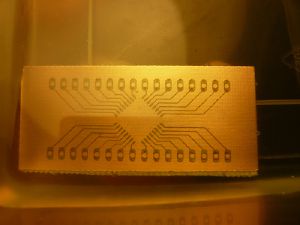
Follow instructions on the notice, but the board is done when all the exposed copper is removed. The balance is removing too much copper and getting breaks in traces vs not enough and some small closely laid traces may have bridges. You are looking for clean edges to your traces - not wobbley "chewed" looking edges (which could indicate you etched for too long, not long enough, or that your exposure wasn't crisp enough). This can take anywhere between 10 and 30 minutes.
After this stage you should rinse the board in water for at least 60 seconds (using the integrated spraying slots in the etching station) before touching it with your hands, transferring to the next tank to begin stripping the photo resist.
Stripper
The stripper is in Tank C
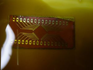
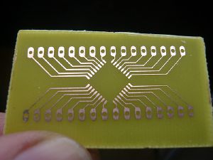
The stripper removes the photo-resist left over after etching. Use the stripper for the specified time then scrub the black off and you should have nice copper traces! Use a multimeter to check for bridges.
After this stage, you may want to rinse the PCB in clean water using the integrated spraying slots, and then IPA.
Milling / Drilling
Normal drill press probably not ideal (not immune enough to wandering!).
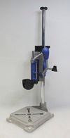
You could use the Dremel stand (on the shelf outside the wood workshop) to drill holes more precisely.
May not have the original dremel, but other (green and blue) rotary tools fit as well.
At this point, you could do any number of finishing options (milling, tinning, soldermask, silkscreen, laquer etc etc). But to aid in the application of solder, you may want to give it a quick brush with some steel wool.
Test / Assembly
If you're doing a double sided board, you'll need to solder up your vias first (we have no through hole plating facilities). A bit of solid core wire works well for this.
See also
More info on the process, including photos of an SMT breakout board
Results people found with materials/compounds
| Name | Date | PhotoResist source (Rapid photo resist spray/pre sentesized deluxe board?) | UV exposure stencil used (paper/acetate?) | Exposure time (minutes) | Develop time (minutes) | Etch time (minutes) | Notes |
|---|---|---|---|---|---|---|---|
| mentar | 14/10/2014 | Kelan presentesized | Transparency | 3 | 1-2 | 8 | Debugging issues with microtrack boards |
| mentar | 3/4/2014 | Farnell presentesized epoxy glass FR4 board | Plain paper | 2 | 5 | 12 | First run in the new space |
| Miguel | 13/5/2014 | white, single sided presentesized board (space stock) | Laserable acetate supplied and printed on by local printshop (£1.50) | 3 | 1.5 | 8 | Professionally printed acetate |
| jasiek | 19/06/2015 | Generic PCB from eBay | Xerox Performer universal paper | 15 | 0.5 | 20 | Did not work. Paper blocking UV? |
| jasiek | 19/06/2015 | Generic PCB from eBay | Laser acetate sheet | 5 | 0.5 | 20 | Worked great |
| levidhuyvetter | 02/08/2015 | KELAN 141300 PCB | Plain paper from laser printer | 6 | 5 | 18 | With fresh developer. |
