Project:PCB Making: Difference between revisions
Danielsikar (talk | contribs) |
Danielsikar (talk | contribs) |
||
| Line 88: | Line 88: | ||
* Preparing for exposure. Double-up transparency for better results. | * Preparing for exposure. Double-up transparency for better results. | ||
[[File: | [[File:Developing_photoresist.jpg|400px]] | ||
* Peeling off protective layer. | * Peeling off protective layer. | ||
Revision as of 14:02, 12 May 2010
Project maintained by Daniel Sikar ~/ dsikaratgmaildotcom.
Project Brief
Summary
How to make a Printed Circuit Board (PCB) using photoresist laminates.
Overview
This howto is intended as a module, aimed at providing building blocks to emulate and extend projects such as Benito and Nanduino.
Motivation
PCB making autonomy, although not an absolute necessity in this day and age, is helpful.
Once an electronic prototype is working on a breadboard, the next logical step is to firm up all components on a PCB, where they are less likely to come apart.
Bringing electronic designs to life engenders spatial awareness and can also be fun.
The bigger picture
There are several steps in producing electronic devices. PCB making comes in after the artwork is ready to be transferred and before the components are ready to be soldered onto the board.
Method
The method described consists of exposing, developing, etching, drilling and tinning a photoresist copper-clad board.
Bill of Materials (BOM)
- Photoresist Copper-clad board Maplin product page (code FA61R).
- Sodium Silicate Maplin product page (code AP01B).
- Ferric Chloride Maplin product page (code XX12N).
- Methylated spirits Wickes product page (code 600343).
- Flux pen Maplin product page (code N63AA).
Additionally:
- Scale
- Tubs
- Mixing and storing vessels
- UV exposure box
- Hammer & punch
- Drill & drill bits
Steps in a nutshell
Note in this cross section, black in the transparency layer represents a via (trail) on the left and a pad (where a component pin will be soldered) on the right.
1. The artwork (printed onto a transparency) is placed over the photoresist copper-clad board and exposed to UV light. (8 minutes)
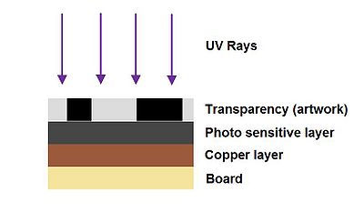
2. The photo sensitive coating weakens as a result of exposure, and is rinsed off with a 10% Sodium Silicate solution. (1-2 minutes)

3. Copper-clad board is immersed in a 30% Ferric Chloride solution until etched. (30-40 minutes)

4. Remaining photo sensitive coating is removed with Methylated spirits. This can also be achieved by scrubbing the etched board with wire wool.

5. Board is drilled to allow mounting of Through Hole (TH) components.

6. Flux is applied to copper, which is then tinned.

An additional step is to coat the finished board with an insulating layer which prevents short circuits in case of conductive objects coming in contact with the copper trails. This can be distinguished by a varnish (often green) finish, seen in commercial PCBs.
Real life example
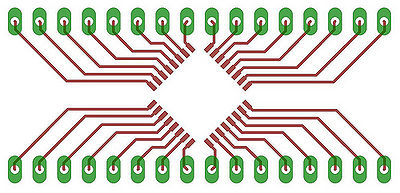
- Artwork, generated by the popular CadSoft Eagle package (.brd file, "top" and "pad" layers shown).
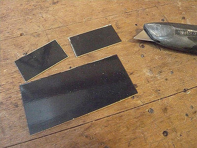
- Cutting board to size, by scoring and snapping.
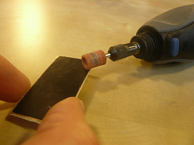
- Finishing the edges, to ensure good contact between transparency and board.
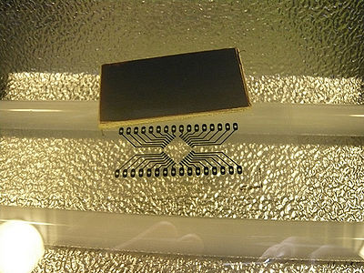
- Preparing for exposure. Double-up transparency for better results.
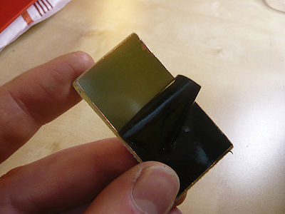
- Peeling off protective layer.
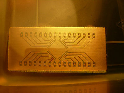
- Developing the photoresist in a Sodium Silicate solution.
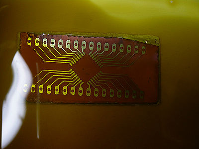
- Etching.
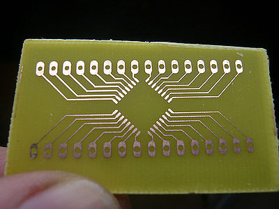
- The etched board.
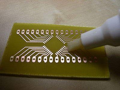
- Applying flux.
Notes
Artwork can be printed straight onto a transparency sheet, on a laser printer. Alternatively high street print shops will do the job.
The board was drilled on the Dremel Workstation. Drill bit; 0.7mm (smallest one) on the workstation plastic drill case, chuck is in the silver dremel case.
The UV box is kept on the floor, diagonally opposite the "rainy shelf" corner.
The chemicals and tubs are on the rainy shelf, next to the coffee maker.
If anyone in interested in making PCBs and needs a hand, let me know.
