Guides/PCB Fabrication
This is a guide on generally how to get PCBs fabricated. It is NOT a guide on how to etch PCBs - that's the PCB Etching Instructions page.
Introduction
There comes a time when an electronic circuit just needs something a bit more permanent to be built on. That's when you will want to build a PCB.
Design
Before you can make your PCB, you'll have to design it. You'll need to do this with some CAD software - there are a few out there, some are "free" and some are free software.
These packages often have quite a steep learning curve, so you may need to invest some time into learning them for the first time.
EAGLE CAD
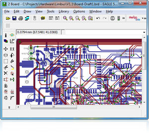
EAGLE is a low cost, hobbyist friendly bit of software that allows you to do schematic capture and PCB design. There is a freeware version, with some limitations on what you can do. The Hobbyist license costs £120. The layout area is restricted to a maximum of 160mm x 100mm (6.3inch x 3.9inch), a schematic can consist of a maximum of 99 sheets and a maximum number of 6 signal layers are allowed. Many thousands of components in Farnell's catalog are associated with EAGLE libraries.
There are a number of tutorials available on the Cadsoft website and also youtube
SparkFun have a lot of excellent EAGLE tutorials which can help you get started.
Project:PCB_Design_with_Eagle_CAD
KiCad
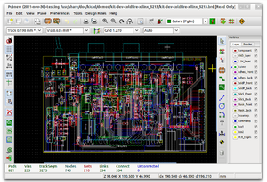
KiCad is an EDA software suite for the creation of professional schematics and printed circuit boards up to 16 layers. KiCad runs on Windows, Linux and Apple OS X and is released under the open-source GNU GPL v2 free of charge.
The particularly useful thing about KiCad is that it is entirely unlimited, and also free. This means you can design 4 layer boards without having to buy any (possibly restrictive) software licenses. It's extremely powerful, but somewhat unorthodox.
There is a full Getting Started guide on the KiCad website, as well as various tutorials on youtube to help you get started.
DesignSpark PCB
DesignSpark PCB is free, has unlimited schematic sheets per project, up to 1m squared of board size and no limits on layers. It can be used for schematic capture, PCB board design & layout, generating 3D views, and generating manufacturing files. Where appropriate, generating a Bill of Materials (BOM) report gives RS Components order numbers.
Fritzing
Fritzing is open source, free software, devoted to making creative use of electronics accessible to everyone. It can be seen as an electronic design automation (EDA) tool for non-engineers. It uses a breadboard prototyping as the design basis.
DipTrace
DipTrace offers schematic capture, PCB layout, component library creation and 3D modeling. There is a free version, DipTrace Lite which allows 500 pins and, 2 signal layers. Also it does shape-based auto-routing for optimizing length of traces.
Fabrication
Once you have finished your design, you'll want to actually make the board!
Etching in the space
The space has some etching facilities, for which you can view the instructions here: PCB Etching Instructions.
Be warned, though, there are no tinning, through hole plating, silk screening facilities. It's great to get you by for a quick turnaround prototype, but for anything more fancy, you'll probably want to send your design off to the professionals.
Professional Fabrication
To get that lovely shiny looking PCB you're after, you can send off the design to a fabrication house to have it made for you.
Processes
Copper Pour
This is the copper which makes up your circuit. The process starts with a copper clad board, which has a thickness of copper denoted by the weight of copper spread over a 1 ft square area (in Ounces). Typically this is 1 oz for external layers, and less for internal layers.
1 oz equates to 1.37 mils (thousandsth of an inch) or 0.0347 mm [1]. The width scales up rectiliniarly, so 2 oz is twice the width of 1 oz, etc.
If your design has critical dimensions for your tracks, you might want to double check the thickness available to you before starting the layout.
Soldermasks
Soldermasks are a coloured coating that goes over your board that prevents solder from flowing into bits that you don't want solder to flow. Traditionally, this is a darkish green colour (which is what primarily makes PCBs look so green!) - however there are a variety of different colours available. Some fab houses will do boards without soldermasks and silkscreen cheap (or maybe even free) - but bear in mind that a soldermask is important for components with a fine pitch (SMT, mainly) as it will prevent shorts between pins.
Silkscreen
This is the (usually) marking you see on the boards with component identifiers and the like. This is purely decorative, and isn't usually applied as precisely as the other layers - so you may get slight registration errors. Silkscreen has to be applied over a soldermask - it will not adhere to exposed copper or board.
Plated Through Holes
When you want to get a signal from one side of the board to another, you'll need a via. This is just a pad which is drilled through to both sides of the board, with an electrical connection between the pads. If you're etching a board yourself, you'll need to make this connection yourself using a small bit of wire, or a rivet.
PCB fabrication houses provide a way of electroplaying the holes (plated-through holes (PTH) [2] ) such that they make the connection without needing any extra processing [3].
Finishing
Once the PCB has been etched and soldermask applied, a number of different finishing processes may be used to improve the quality of the board.
Hot Air Solder Levelling [4] involves the PCB being dipped into a solder bath - which wets the exposed copper with solder. You can get this in tin/lead or lead-free compositions. This provides a good solderable finish, but possibly not completely flat pads (especially for large areas).
Immersion Silvering [5] [6] [7] involves depositing a thin layer of silver onto your PCBs contacts. This produces a much flatter result than HASL, and even better wetting. But it can be a bit more expensive.
Gerber files
Most fabrication houses will accept "industry standard" Gerber files. You'll need to find out how to generate these in your CAD software, and what the specifications of the files are from your fabrication house. They'll normally require a standard subset of files (layers) for top and bottom copper, silkscreens, drills and holes.
Once you've generated these files, you should load them into a gerber viewer (like gerbv) to check them before you send them off!
Fab Houses
There are a number of places which can fabricate your board, here are some possibilities
- UK/EU commercial suppliers. Fairly expensive but can be fast and good quality.
- Spirit Pretty well priced. Also provide a free & fast 'Naked' PCB service [8] (though they do put advertising around your board, and they won't cut it to shape for you)
- Stickleback [9]
- Ragworm.eu (owned by Stickleback) hobbyist centric service
- Eurocircuits EU based PCB house - several proto services. Fairly cheap for stainless SMT stencils.
- PWT UK based full-capability PCB place for stuff Screenbond can't do. Typically cheaper than Eurociruits for 4-layer
- Screenbond UK based PCB house with unusually low tooling costs (typ £40). 1 & 2 layer only. Can do 24hr turnround if you have deep pockets.
- PCB-Pool Proto/low-volume oriented PCB service, not the cheapest these days but offer a free stainless SMT stencil.
- PCB Train Fast turn around, good prices. Also have an assembly service and a 1 day (~£40 all in) prototype service for uncoated 2 layer boards.
- Far-eastern suppliers.
- PCBCART PCBs from China. Very cheap once you get over a square foot or two. Reliable, Quality generally good. A gazillion options - funky resist & silk colours
- Seeed Studio Fusion PCB service
- Elecrow
- Gold Pheonix
- Overseas
- OSHPark - out of the DorkbotPDX batch pcb order, and then absorbed Sparkfun's BatchPCB
Comparisons
For some kind of reference for comparison, here is a table of quotes for a fairly standard small board:
- Minimum quantity of boards
- 20x50mm
- 2-layer board
- No particularly coloured silkscreen/soldermask
- Through hole plating
- 1oz copper
- HASL or immersion silvering (whichever is cheaper)
- FR4 1.6mm (or nearest cheapest equivalent).
| Service | Approx Turnaround time | Approx Shipping time | Silkscreen | Cheapest shipping cost | Total quote | Number of PCBs | Cost per PCB (delivered) |
|---|---|---|---|---|---|---|---|
| Ragworm.eu | 10 working days | 2 working days | Orange only | £0.00 (included) | £5.95 | 1 | £5.95 |
| OSHPark see specs | 12 days | 7 - 28 days (average 11 days) | Purple only | £0.00 (included) | £4.50 | 3 | £1.50 |
| PCB Train Express service (no silkscreen, just copper) | 2 days | ? | None | £0.00 (included) | £30.00 | 1 | £30.00 |
| PCB Train 2 layer (with soldermask and silkscreen) | 10 days | ? | Green only | £0.00 (included) | £44.10 | 1 | £44.10 |
| PCB Pool 2 layer Bare board | 8 days | ? | None | ? | £60.16 | 10 | £6.02 |
| PCB Pool 2 layer (silkscreen + soldermask) | 8 days | ? | Green | ? | £117.30 | 10 | £11.73 |
| ITead 2 layer | ? | 4 - 5 days | Green | £2.29 (Airmail) | £8.10 | 1 | £8.10 |
| Eurocircuits | 25 days | ? | Green | £7.66 (Economy) | £33.02 | 1 | £33.02 |
| Elecrow 2 layer | ? | 7 to 25 days | Various | £2.70 | £8.52 | 10 | £0.85 |
| Seeed Studio Fusion PCB | 5 - 7 days | 0-25 days (Registered airmail) | Green | £4.39 | £10.21 | 5 | £2.04 |
| PCB Snap (Spirit Circuits) | ? | ? | Green? | £10.31 | £61.86 | 1 | £61.86 |
| PCB Cart | 12 days | 3-5 days (DHL) | Green | £17.39 | £59.59 | 1 | £59.59 |
| Gold Phoenix | 5 days | 3 days | Green | ? | £78.96 | 25 | £3.15 |
NB: this is not an endorsement - prices may change, but this could be an indicative guide on roughly how much you might expect to pay.
See Also
- Nottinghack wiki - PCB Suppliers and Manufacturers
- http://en.wikipedia.org/wiki/Printed_circuit_board
- KiCAD Schematic capture + PCB design software
- EAGLE CAD

