LED tiles V2
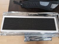
LED screen tiles donated by Tom (Mistamudd) See mailing list thread here.
Specs
The tile contains the matrix of 64 x 16 (1024) RGB LEDs and the driver ICs. Data is sent serially to the LEDs, configured in 'banks' and 'rows'.
Each tile is 500mm wide x 125mm high with LED pixels every 7mm pitch.
There are 48 x MBI5034 LED controller chips on the PCB, which are 16 bit shift register constant current sinks.
Datasheet : File:MBI5034 Datasheet VA.00-EN.pdf
The controller chips are labelled R,G & B 1-16. So each chip does 16 LEDs of the same colour. They each have a current set resistor.
There are two address line inputs and the LED chips seem to be soldered in to banks of 4. Which makes sense.
There is an HC138 decoder on the address lines, and only the first four outputs seem to be wired. Again, matches the above.
There are also 8 dual FET chips, which seem to control the 4 banks.
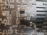
The top connector is all Vcc (5v?)
The bottom is all ground
The middle connector has :
- D1 & D2
- OE (Output enable)
- LAT (Latch)
- A0 & A1
- CLK (Clock)
- NC
The serial data sent to D1 & D2 needs to be sent in 3 x 16 bit B,G,R frames, 64 times per row (i.e. one row is 384 bits) then this is latched, and then the output is enabled.
BBBBBBBB BBBBBBBB GGGGGGGG GGGGGGGG RRRRRRRR RRRRRRR | BBBBBBBB BBBBBBBB GGGGGGGG GGGGGGGG RRRRRRRR RRRRRRR | BBBBBBBB BBBBBBBB GGGGGGGG GGGGGGGG RRRRRRRR RRRRRRR ... etc .. x 384 bits
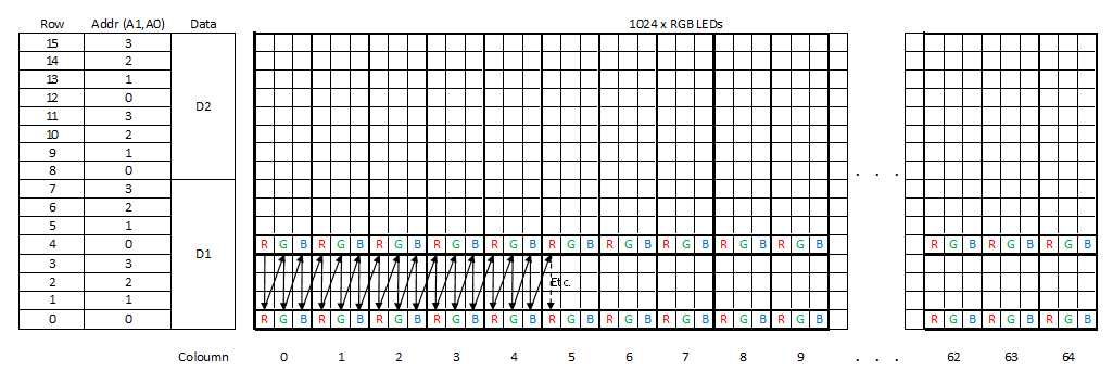
There are two 'banks'; the top 8 rows and bottom 8 rows. There are loaded with data using two different data in lines, D1 & D2. The data lines are clocked and latched with the same shared clock and latch signals.
In each bank, there are 8 rows. A single stream of 384 bits loads two rows of 2 x 64 LEDs. The address lines A0 & A1 select which row is being loaded from the serial data.
To display a full tile, of all 1024 RGB LEDs, you need to :
- Set OE=HIGH & LAT=LOW
- For each address A0 & A1 = 0x00. 0x01. 0x10. 0x1 :
- Clock 384 bits of data on to D1 & D2, by toggling the CLK pin from LOW to HIGH
- Toggling LAT pin from HIGH to LOW to latch the 384 bits in to the driver chips.
- Toggle the OE pin LOW to turn the LEDs on for that row.
Repeat this very quickly as fast as you can ! :-)


